Customized premium Forex VPS for successful traders. Our goal is to ensure that any complex automated trading can be handled with our dependable top VPS Forex solutions.
400+ Active Subscribers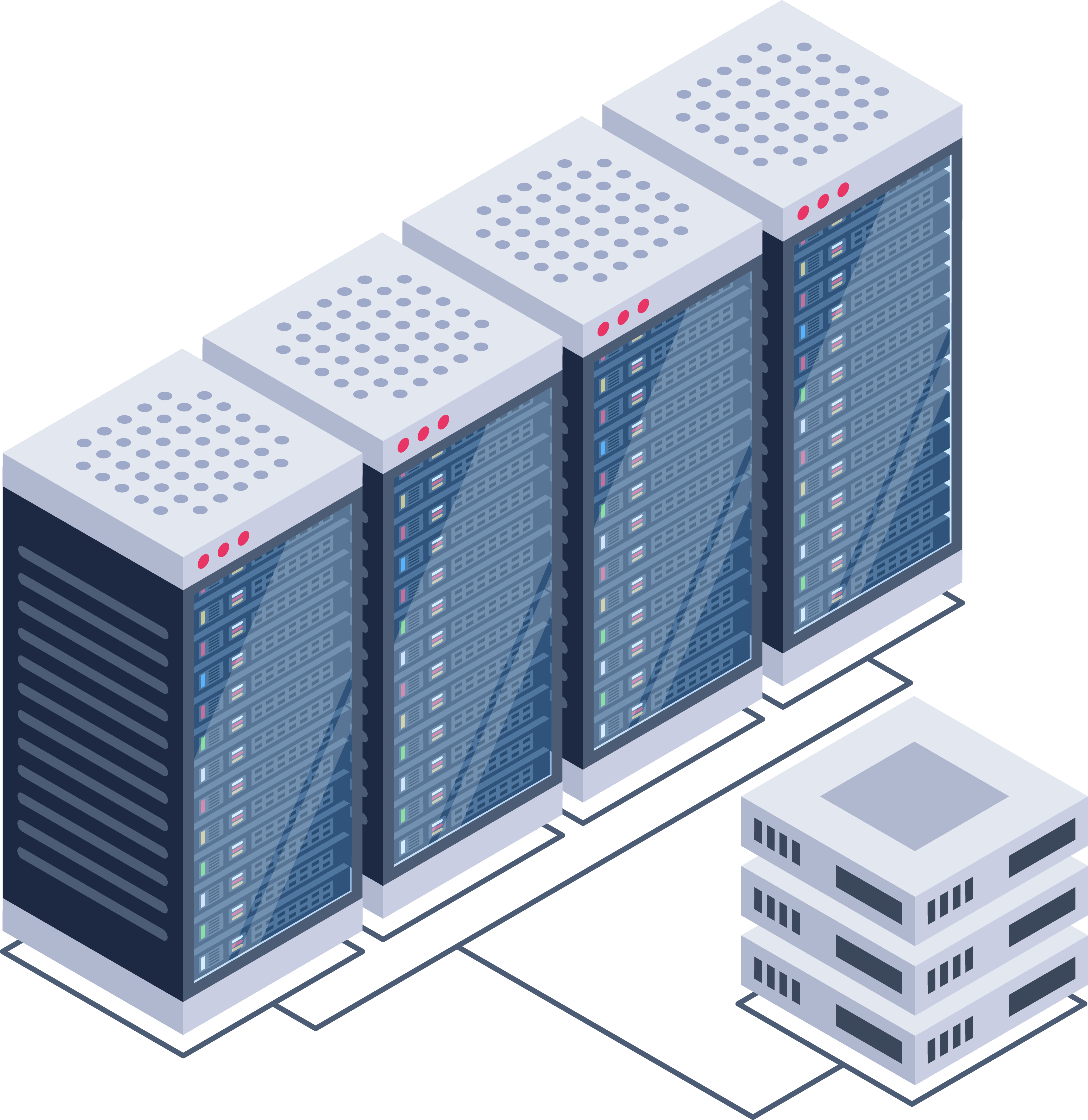
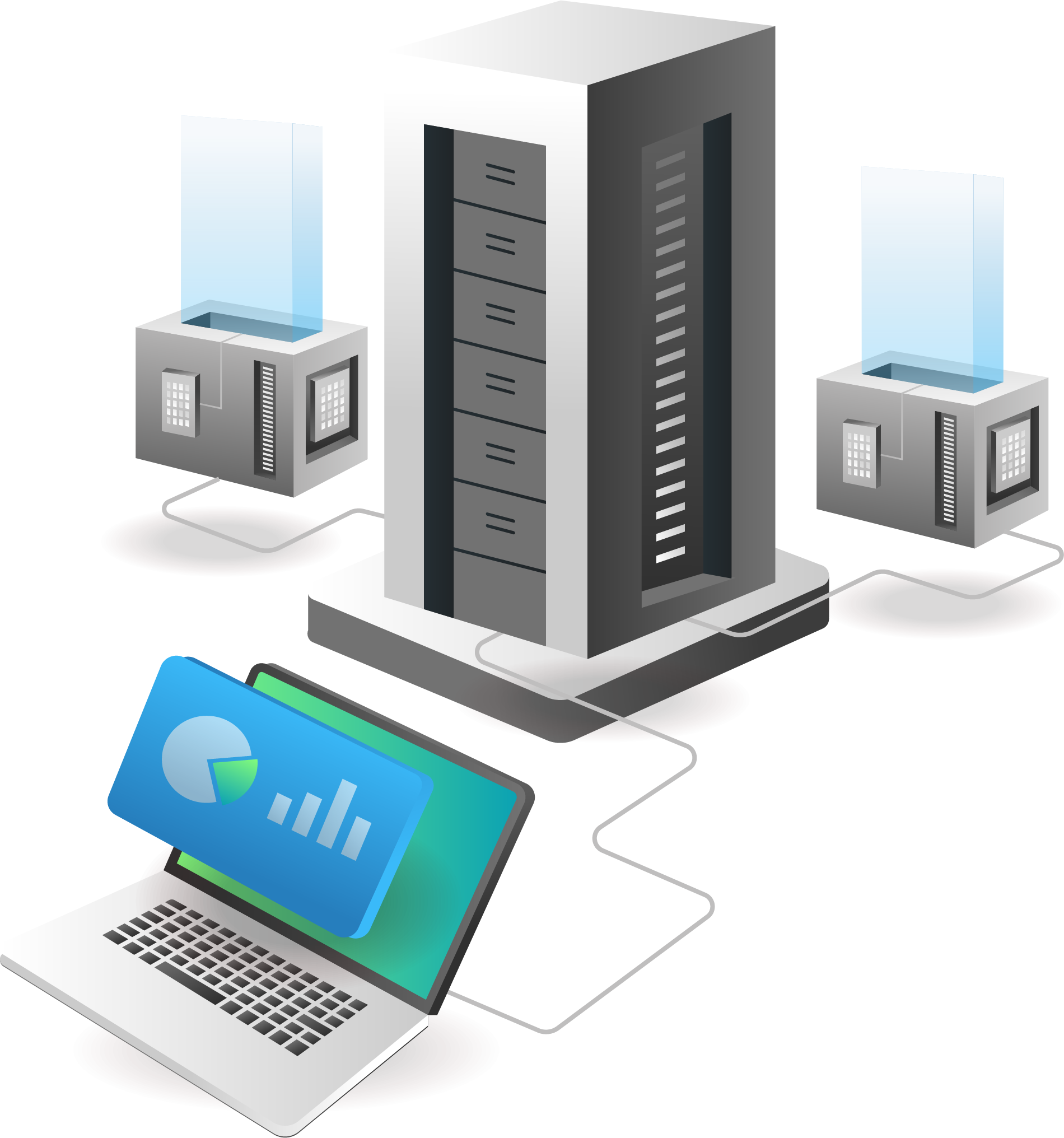
Our VPS servers, colocated in financial data centers, deliver ultra low latency and fast execution speed for forex trading.
per month
per month

Utitlize our PAMM Strategy for completely hands off results .
VPS Subscribers
MM USD Managed

Step by step guide on how to setup your MT4 Terminal so you can start trading today.
Market Maker Strategy Made Easy (coming soon*)